UB and SUNY Erie to advance workforce development in microelectronics

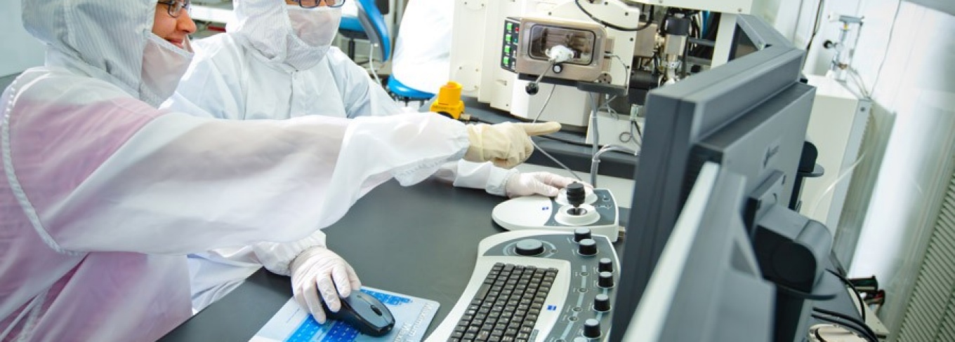
UB’s cleanroom, above, is one of the most advanced in Western New York, complete with nanolithography, deposition and etching capabilities.
By Peter Murphy
Release Date: March 25, 2025


BUFFALO, N.Y. – The University at Buffalo and SUNY Erie Community College – and their cleanrooms – are teaming up to boost workforce development and education in the microelectronics and semiconductor industry.
Both institutions will expand UB’s Cleanroom Fundamentals course, into an online experience. This partnership will deliver a full spectrum of microelectronics education and also help the institutions secure state and federal funding for microelectronics research.
Educating the future workforce
UB, a long-time leader in semiconductor and microelectronics research and education, launched the Center for Advanced Semiconductor Technologies in 2024 shortly after the Buffalo-Rochester-Syracuse region was designated a federal tech hub following the passage of the CHIPS and Science Act – a $280 billion effort to boost microchip research and production in the United States.
The Center for Advanced Semiconductor Technologies, The Center for Industrial Effectiveness (TCIE) and SUNY Erie are joining forces to offer a new digital version of UB’s Cleanroom Fundamentals course. The course provides students interested in a STEM career with insights into semiconductor manufacturing and technologies.
“We’re excited about this opportunity to partner with the University at Buffalo to bring the Cleanroom Fundamentals Course to SUNY Erie. The implementation of the course at our college is in the planning stages; once complete, we plan to offer the course through our Office of Workforce Development,” said SUNY Erie President Adiam Tsegai. “At SUNY Erie, we foster many partnerships such as this one that help ensure academic success for our students and those who participate in our workforce development programs.”
This new online course features a digital hands-on lab component, giving students the full experience of being in the cleanroom. In addition to the lecture and learning the concepts associated with the cleanrooms, students will fabricate a patterned wafer using photolithography and etch technologies.
UB and SUNY Erie are working with Micron Technology, Inc., one of the world’s largest semiconductor manufacturers to develop the course.
“Our ultimate goal is to enlarge the United States semiconductor workforce pipeline,” says Timothy Leyh, executive director of TCIE. “By leveraging UB’s funded and proposed programs, we will use Micron’s gift to scale this course, and encourage students already interested in STEM to pursue semiconductor occupations by bringing into focus the global, social and environmental issues the technologies can address, as well as the career potential.”
Micron is building a 1,400-acre semiconductor fabrication facility in New York State that will create nearly 50,000 New York jobs. The U.S.-based corporation will build the largest cleanroom in the nation, in another step toward addressing the demand of consumer, industrial and business products.
“The semiconductor industry is undergoing a remarkable renaissance at present and the demand for a skilled workforce to support this progress is only expected to grow over time,” says Jon Bird, director of the Center for Advanced Semiconductor Technologies, and professor and chair in the Department of Electrical Engineering. “Together, with Micron and SUNY Erie, we are dedicated to creating valuable learning experiences that bridge the gap between academia and industry.”
Leveraging unique spaces in Buffalo
UB’s cleanroom is one of the most advanced in Western New York, complete with nanolithography, deposition and etching capabilities – all critical processes in semiconductor fabrication. The cleanroom, located on UB’s North Campus, also provides project consultation, workforce training/education and several other services.
SUNY Erie’s cleanroom, located in the Center for Nanotechnology Studies on the college’s North Campus, is one of the only community college-hosted cleanrooms in New York State. Its technology can manipulate particles within an advanced manufacturing process.
UB and SUNY Erie aim to have the course live during fall 2025.
Media Contact Information
Media Relations (University Communications)
330 Crofts Hall (North Campus)
Buffalo, NY 14260-7015
Tel: 716-645-6969
ub-news@buffalo.edu